Material Characterization Techniques Using the Keck Microanalysis Laboratory

Dr. Sara Kassis
Lecturer
ES Department, Sonoma State University, Rohnert Park, CA
Thu, 04/21/2016
Abstract – Characterization techniques are essential to observing behavior and properties of materials. It is especially useful to investigate the structural and surface properties of materials at the microscopic level since the behavior in this regime dominates our current technology using semiconductors, which are the key components in making digital processors found in computers and other devices function. This talk will focus on how the instruments in the Keck Microanalysis Laboratory at SSU can be utilized to investigate properties of materials.
Dr. Kassis received her PhD in Condensed Matter Physics from Kent State University. Her experience includes over 10 years of teaching physics and engineering at various universities. Her research interests include materials engineering and characterization, nanomaterials, and low temperature physics.
FTTX: Key Market and Technology Trends
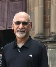
Dr. Rajiv Dighe
Sr. Product Line Manager
Broadcom
Thu, 04/07/2016
Abstract – World-wide broadband access deployments have seen massive growth due to fiber access technologies based on Passive Optical Networks (PON). In this talk, we describe the different PON technologies that have been currently deployed (IEEE-based EPON, ITU-based GPON) and the next generation higher bandwidth solutions (IEEE-based 10G EPON and ITU-based XGPON1, NGPON2). We also talk about the market drivers for these technologies as well as the different deployment models (Fiber To The Home, Fiber To The Curb, Fiber To The Basement etc.). Lastly we illustrate how these technologies will be the building blocks of the Digital Smart Home as we move to the Internet of Things.
Mr. Rajiv Dighe got his Ph.D in Electrical Engineering from University of Notre Dame in 1986. He started his career at ATT Bell Labs working on Broadband Networks. A Broadband Systems Architect with more than 30 years experience in architecting and building packet based (ATM/IP) platforms for next-generation networks as well as Digital Subscriber Loops (DSL) and Passive Optical Networks (PON) chipsets. He holds 22 US Patents and currently manages the xPON-based Home Gateway SoCs for Broadcom.
THz Interconnect, the Last Centimeter Communication (2016)
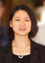
Dr. Jane Gu
Assistant Professor
Electrical and Computer Engineering, UC Davis
Thu, 03/10/2016
Abstract – Ever increasing chip-to-chip communication bandwidth requirement continuously exceeds the bandwidth capabilities supported by chip I/O pins. The gap between the interconnect requirement and the capability forms “Interconnect Gap”. This talk presents one potential scheme, THz interconnect, to address the “Interconnect Gap” challenge. THz Interconnect, leveraging its unique spectrum position, holds the potential to utilize the benefits of both electrical interconnect’s low cost, high scalability processes and optical interconnect’s low loss channels. Therefore, it is promising to boost all the three key metrics of interconnect: bandwidth density, energy efficiency, and low cost, to address the long-standing issue. This talk presents THz interconnect active, passive component design and system demonstration.
Dr. Q. Jane Gu received her Ph.D. degree from University of California, Los Angeles in 2007. After graduation, she has worked in the industry for a short period. From August 2010 to August 2012, she was an assistant professor at University of Florida. Since August 2012, she has joined University of California, Davis as an assistant professor. Her research interest includes high efficiency, low power interconnect, RF/mmwave/ THz integrated circuits and System on Chip (SoC) design techniques, as well as integrated THz systems for communication, radar and imaging. She is the co-recipient of 4 conference best paper awards. She is the recipient of 2013 NSF Career Award and 2015 College of Engineering Outstanding Junior Faculty Award.
Optical Coherence Tomography - Lighting the Path to Better Healthcare

Dr. Audrey Bowden
Assistant Professor
Electrical Engineering, Stanford University
Thu, 03/03/2016
Abstract – Cancer. Infertility. Hearing loss. Each of these phrases can bring a ray of darkness into an otherwise happy life. The Stanford Biomedical Optics group, led by Prof. Audrey Bowden, aims to develop and deploy novel optical technologies to solve interdisciplinary challenges in the clinical and basic sciences. In short, we use light to image life -- and in so doing, illuminate new paths to better disease diagnosis, management and treatment. In this talk, I will discuss our recent efforts to design, fabricate and/or construct new hardware, software and systems-level biomedical optics tools to attack problems in skin cancer, bladder cancer, hearing loss and infertility. Our efforts span development of new fabrication techniques for 3D tissue-mimicking phantoms, new strategies for creating large mosaics and 3D models of biomedical data, machine-learning classifiers for automated detection of disease, novel system advances for multiplexed optical coherence tomography and low-cost technologies.
Dr. Audrey K (Ellerbee) Bowden is an Assistant Professor of Electrical Engineering at Stanford University. She received her BSE in EE from Princeton University, her PhD in BME from Duke University and completed her postdoctoral training in Chemistry and Chemical Biology at Harvard University. During her career, Dr. Bowden served as an International Fellow at Ngee Ann Polytechnic in Singapore and as a Legislative Assistant in the United States Senate through the AAAS Science and Technology Policy Fellows Program sponsored by the OSA and SPIE. She is a member of the OSA, a Senior Member of SPIE and is the recipient of numerous awards, including the Air Force Young Investigator Award, the NSF Career Award and the Hellman Faculty Scholars Award. She is a former Associate Editor of IEEE Photonics Journal, a member of numerous professional committees, and her research interests include biomedical optics, microfluidics, and point of care diagnostics.
Bleeding Edge FPGA and Digital Design: New Challenges At High Gigabit Rates
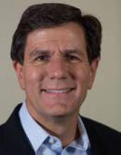
Mr. Chuck Corley
Principal Digital HW Engineer
National Instruments
Thu, 02/18/2016
Abstract – Today's ASICs and FPGAs include multi-gigabit data transceivers that operate at 28 Gigabits per second. Future 56 Gigabit per second links are being designed and will arrive soon. Problems have been encountered in making these new data links reliable. The physics of PC Board signal transmission at these rates is the next high frequency challenge for digital and signal integrity engineers. This presentation investigates these latest challenges and some of the proposed solutions.
Mr. Chuck Corley is a multi-discipline 'crossover' hardware and software engineer who enjoys the challenges of making new technologies work reliably. Some of his current engineering passions include Field Programmable Gate Arrays (FPGAs) and ultra high speed multi-gigabit digital design signal integrity. Chuck has Bachelor's and Master's degrees in Electrical and Electronic Engineering from Sacramento State University. Chuck is proud to have worked for Hewlett Packard, Agilent, Cisco, Mahi Networks, and Keithley Instruments. Currently he feels very privileged to be part of the team at National Instruments, and also teaches high speed design classes. Chuck's latest hobby is being a project lead for Engineers Without Borders, designing and building sustainable clean drinking water systems for native villages in the Amazon region of Peru.