An International Teaching Experience: Challenges and Rewards
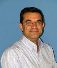
Dr. Farid Farahmand
Assistant Professor
Engineering Science Deptartment, SSU
Thu, 11/21/2013
Abstract - In this talk, we explore the challenges and rewards of teaching overseas. We share some of our personal experiences during our 7-month stay in Ghana and point out the difficulties facing academic institutions in the country. We examine opportunities for introducing new technologies to improve the education system in developing countries. We further recount on the importance of "appropriate" technologies aiming at improving the standard of living for the developing world. We offer personal accounts as to how such technologies can greatly impact living conditions of many people and how students, particularly STEM majors, can be engaged in collaborative multidisciplinary international projects involving humanitarian technologies. Finally, we conclude by presenting available volunteer opportunities for faculty and students to visit West African countries and potential contributions they can make, while experiencing the incredible natural beauty, cultural richness, and human kindness in the region.
Dr. Farid Farahmand received his PhD in 2005 and is currently an Assistant Professor in the Department of Engineering Science at Sonoma State University. He is also the director of Advanced Internet Technology in the Interests of Society Laboratory. Prior to this position, Dr. Farahmand worked as the research scientist at Alcatel-Lucent Corporate Research and was involved in development of terabit optical routers. Dr. Farahmand holds multiple international patents, numerous reference conference articles and journal publications, and several book chapters, on the subjects of wireless communications, optical networking, green networking, and delay tolerant networks. He has also authored many educational papers focusing on eLearning and Active Learning in classrooms. Farid is actively involved in many conferences and serves as the reviewer and co-editor to a number of technical conferences and journals. He is a member of IEEE, ASEE, and Engineers Without Borders-USA.
Electrochromic Windows Based on Reduction /Oxidation Reactions: A Review
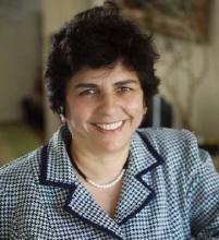
Dr. Nilgun Ozer
Director of Student Resource Center and MESA Engineering Program
SFSU
Thu, 11/07/2013
Abstract - Electrochromic (EC) windows for buildings offer substantial benefits by increasing the thermal and the visual comfort of the occupants and simultaneously reducing the energy consumption in the buildings. EC windows can be reversibly switched from a transparent colorless state to a more opaque state by applying an electric voltage. These windows will be key contributors towards advanced building technologies which will conserve the World energy resources. EC system designs for glazing include solid state layers, and ionically conductive polymer. A typical EC window consists of two glass sheets coated with transparent conductors, which are coated with the active solid state layers. The two sheets are laminated together with an ionically conductive polymer. These are all based on absorptive technology which does not completely resolve issues such as re-radiation of energy back into the building or privacy. This presentation summarizes the EC properties of smart window glasses and its applications.
Dr. Nilgun Ozer received her bachelor’s degree in 1976 from Istanbul University, master’s degree in 1978 from Bogazici University, and earned her Ph.D. in 1983. She currently holds a director of Student Resource Center and MESA Engineering Program position in the College of Science and Engineering at the San Francisco State University. Dr. Ozer is an editorial board member of Journal of Solar Energy and Materials and American Journal of Engineering Education. She also serves as faculty advisor for the Collegiate chapters of Society of Hispanic professional Engineers (SHPE), National Society of Black Engineers (NSBE) and Society of Women Engineers (SWE). She has 25 years of teaching and research experience at different universities and research institutions in Europe and the United States. Dr. Ozer also worked as a consultant in science and engineering education for United Nations Educational Scientific and Cultural Organization (UNESCO) from 1989 to 1993. Dr. Ozer’s research interests are applications of wet chemical deposition techniques for optoelectronic thin films in the field of renewable energy such as electrochromic devices, solar cells, and solar panels.
Developing Environmental Sensor Networks at the SSU Preserves: Opportunities for Cross-Disciplinary Collaboration
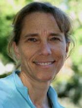
Dr. Claudia Luke
Director of Field Stations and Nature Preserves
SSU
Thu, 10/17/2013
Abstract – Advances in sensor, communication, and computing technology are transforming understanding of environmental processes on a global scale. Despite the promise that new cyber-technologies hold, much more research and training are needed to advance this new field. Unfortunately, student access to networks needed for real-world experiences is typically limited at undergraduate institutions. The SSU Preserves is working with Farid Farahmand and other faculty in SSU’s Engineering Science Department to construct a wireless sensor network at the Fairfield Osborn Preserve. The project builds on existing senior capstone projects and Master’s degrees to create a small high-speed wireless network that: (a) Collects and transmits sensor data that can be used by classes on campus, (b) Interfaces with sensors and software designed by engineering and computer science students, (c) Introduces students in other disciplines to fundamentals of engineering, instrumentation, and measurements needed for a technologically literate society, (d) Creates opportunities for professional employment experiences for Engineering Science students.
Dr. Claudia Luke, Director of SSU Preserves, earned her Ph.D. in Zoology at UC Berkeley. She has 20 years of experience directing 6 university field stations for the University of California and California State University systems. She has worked extensively with partners and collaborators to build regional research, management, and education collaborations in the areas of watershed management, fire management, habitat connectivity, and habitat enhancement. As Reserve Director for San Diego State University, she supported the development and use of a 4,000-acre wireless sensor network, which included obtaining a $1.2 million collaborative grant to explore the efficacy of fire sensors in enhancing community safety.
High Frequency Design On PCB
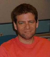
Mr. Tamir Moran
Principal Hardware Engineer
National Instruments
Thu, 10/03/2013
Abstract – The growing consumer wireless market continues to demand ever increasing performance at lower cost, shorter design cycles, and smaller size that challenge engineers in ways never seen before. To enable this fast growth of wireless devices, Test & measurement (T&M) companies must stay ahead of the technology deployment curve and routinely deliver high performance test solutions at compelling price points. Previously, RF/Microwave design relied on long prototyping cycles, exotic materials and sophisticated processes that were unsuitable for meeting aggressive design cycles and cost goals. Modern RF Engineers depend on improved modeling techniques, simulation tools like AWR, off the shelf components, and wellknown, cost effective manufacturing processes to meet the timeframe and high volume demands of component vendors. In the last decade, The availability of RFICs in surface mount (SMT) packages and high volume, high frequency PCB technologies have emerged to allow engineers to meet market demands for performance, cost and schedule. This presentation will discuss a design cycle that combines highly advanced simulations available in AWR with the latest PCB process to show RF/Microwave engineers a new methodology to meet their performance, cost and schedule goals.
Mr. Tamir Moran received his BSEE and MSEE in 1997 and 1999, respectively, from the University of Arizona, Tucson. In 1999 he joined Agilent Technologies as a design engineer in the Network Analysis Division, Santa Rosa, CA, where he designed high frequency circuits on PCB and hybrid circuit technologies. Since 2006 he has been with National Instrument’s R&D center in Santa Rosa, CA working as a Principal RF Engineer developing RF/Microwave PXI modules for the Test & Measurement Industry, and responsible for developing advanced technologies.
Design and Testing Challenges of Consumer Devices in High Volume Manufacturing
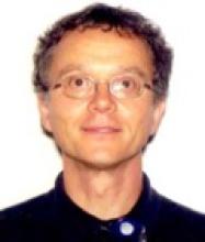
Mr. Bela Szendrenyi
Senior R&D Design Consultant
Advantest America Inc.
Thu, 09/19/2013
Abstract – Ever wondered how can be cell phones and other electronic gadgets produced so inexpensively that service providers are giving those away for just about a few Dollars? One example is a recent iPhone3 deal for 99 cents… Even if some cost is recovered with monthly locked-in fees, production cost is counted barely 18-23% of actual consumer price. So how are these complicated Silicon chips manufactured and fully tested for under a Dollar? Ever increasing system requirements and mushrooming number of cell channels in USA, Japan, and Europe – require 25-30 different type, altogether few hundred actual measurements done during production of these devices. Consumer expectation is that these phones are fully tested, and all functions work properly. In this presentation we are going to take a quick look at every step of the challenge: automated test system, handler interface, on-wafer measurements, DUT board design, high frequency signal and power integrity! Come and take part of the technical journey the practicing engineer needs to cover in production of these tools of our everyday life.
Mr. Bela Szendrenyi is a lead contributor of the development team in the Test Cell Innovation Group at Advantest America, Inc. He has an MSEE in Telecommunications from the Technical University of Budapest, Hungary. In 1984 Bela joined the Research Institute of Technical Physics for the Hungarian Academy of Sciences where he participated in the high frequency GaAs device development as a Research Fellow. In 1991 he moved to Canada, then few years later to California, where he worked for Gigahertz Technologies, Maury Microwave Inc., Agilent Technologies, and Verigy Inc. companies on various high frequency and high speed programs. Bela and wife, Gyongyi, have two university-age kids and they all live in Santa Rosa. In his free time he likes various sport and outdoor activities, with family.